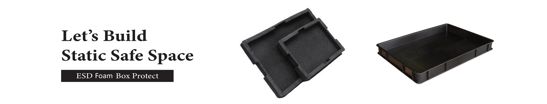
——Precision Anti-Static Foam Solutions Built from 5mm IXPE
✍️ Original article by YUFA Polymer.
�� For inquiry, please contact: info@yufapolymer.com
�� Production Site: Shenzhen, China
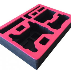
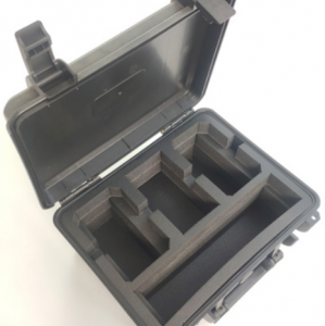
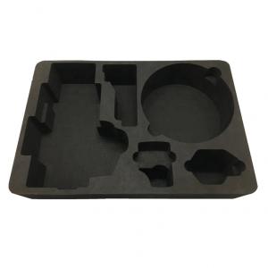
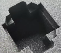
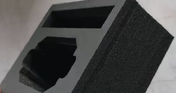
Built from 5mm anti-static IXPE foam layers, we design and manufacture custom-shaped ESD foam inserts to securely hold, protect and handle semiconductor devices.
From simple cavities to complex multi-layer structures, our foam inserts are engineered to fit your ICs, modules and sensitive components precisely — reducing movement, minimizing ESD risk and improving handling efficiency.
Prototypes ready in 5–7 working days.
�� Get a Custom ESD Foam Insert Quote
Why Semiconductor Devices Require Custom ESD Foam Inserts
In semiconductor manufacturing, testing and transportation, electrostatic discharge, poor positioning and micro-movement can cause irreversible damage.
Standard foam sheets or off-the-shelf packaging often fail to provide:
· Consistent ESD control
· Accurate device positioning
· Structural stability during handling and transport
· Clean, repeatable use in controlled environments
Custom-designed ESD foam inserts solve these problems by matching the exact geometry and handling requirements of your devices.
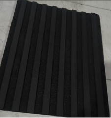
From 5mm IXPE Foam to Precision-Fit ESD Inserts
We start with 5mm anti-static IXPE foam as a modular base, then build your insert structure layer by layer.
This approach allows:
· Controlled thickness from thin supports to up to 300mm total height
· Step cavities, slots and multi-level positioning features
· Better dimensional accuracy compared to single-block foam
By constructing the insert from 5mm layers, we achieve higher consistency, improved structural stability and better cost control for semiconductor applications.
Advanced Foam Processing Capabilities
All ESD foam inserts are produced using in-house processing equipment optimized for IXPE foam:
· CNC machining for precision cavities and pockets
· Die cutting for repeatable, high-volume structures
· Vibration knife cutting for complex outlines and shapes
· Multi-layer lamination and selective peeling
· Custom assembly of layered foam components
These capabilities allow us to manufacture complex, custom-shaped ESD foam inserts reliably and efficiently.
Design Support & Fast Prototyping
With Drawings or Samples
· Send CAD, PDF drawings or physical samples
· Engineering evaluation and confirmation
· Prototype delivered in 5–7 working days
Without Drawings
· Share device dimensions, weight and handling requirements
· Our team designs the foam insert structure for you
· Prototype provided for validation and approval
Whether you have complete drawings or only basic requirements, we help you move forward quickly.
Typical Semiconductor Application
Our custom ESD foam inserts are widely used for:
· IC and chip handling
· Semiconductor module protection
· Test, inspection and assembly trays
· Transport and reusable ESD packaging
· Sensitive electronic component positioning.
Why Semiconductor Customers Choose Us
· Focused on custom ESD foam inserts, not raw foam materials
· Engineering-driven design approach
· Stable anti-static performance and closed-cell structure
· Reliable quality for repeatable production
· Responsive communication and fast turnaround
We work as a solution partner, not just a foam supplier.
Start Your Custom ESD Foam Insert Project
Ready to protect your semiconductor devices with precision-designed ESD foam inserts?
Send us your drawings, samples or requirements today.
Our team will review your project and provide professional feedback quickly.
�� Contact Us Now for a Custom Quote
�� Contact Us
YUFA Polymer Products Co., Ltd.
�� Address: Shenzhen, China
�� Email: info@yufapolymer.com
�� Web: www.yufapolymer.com